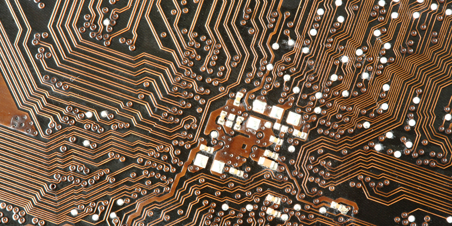
PCB layout
At PCB-Support, we have great expertise in the design of printed circuit boards.
Our experience spans over several market segments, industrial, telecom, datacom, medical and satellite/space among others.
PCB layout is not just about connecting components on a printed circuit board. Depending on the task, many factors may have an influence, for example width of the tracks, isolation distance, via types, signal speeds etc. We work with ”constraint driven designs”, which means that we, in cooperation with the customer, insert the necessary design rules, either on the schematic level or directly in the layout tool. Our software then checks that these rules are respected everywhere on the PCB.
In the case of a PCB design which includes high-speed signals or impedance matching signals, it is very important to have specified the correct PCB stackup. Therefore, we are always in close dialogue with the customer and/or the PCB supplier about this. In this way we ensure a PCB layout of high quality and at the right Price.